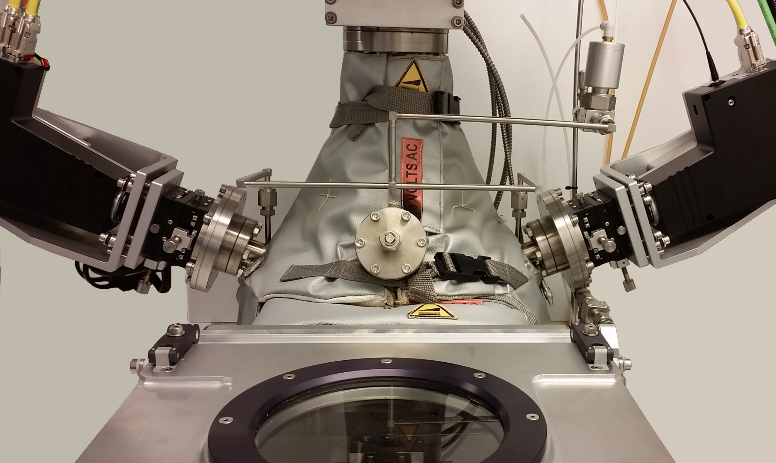
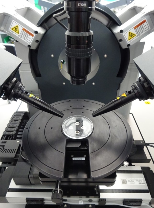
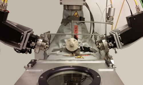
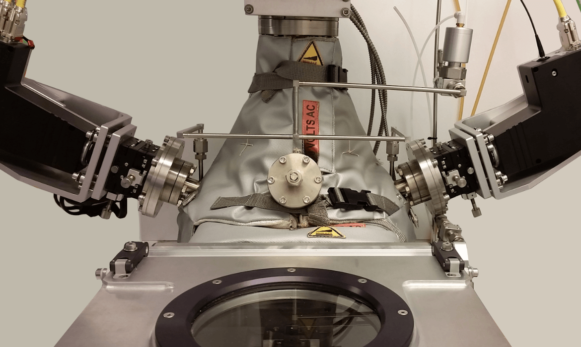
This high-performance, non-contact,non-destructive optical metrology tool provides precise measurement ofthin film thickness and optical constants across single and multilayer structures. Designed for R&D labs, universities, and industrieslike semiconductor, PV and optics, it supports advanced modeling, mapping,and real-time data visualization.

  • Ideal for real-time, in-situ thin film thickness and optical constant measurement; and multilayer stack analysis
  • Used on vacuum chambers during deposition or treatment processes and load locks with in-situ thickness measurement capability
  • Material types:
    • thin dielectric films (oxide, nitride),
    • porous films,
    • very thin metal layers,
    • graphene,
    • 3D nanostructures,
    • organic layers (OLED, polymers),
    • TCOs,
  • Widely employed by universities, R&D labs, PV researchers, optics manufacturers, and pilot production teams

  • High-performance, non-contact, non-destructive optical measurement system for thin films and multilayer stacks
  • Measures film thickness and optical constants (refractive index, extinction coefficient, band gap, composition)
  • Supports scheduled measurements, custom recipes
  • Modern graphical user interface
  • Measurement speed: from ~167 ms up to several seconds (typically 1–10 seconds)
  • Wavelength range: 245 nm – 990 nm
  • Minimum integration time: 167 ms
  • Beam divergence: <0.06°
  • Angle of incidence: 70° oin testbench
No items found.
inSE-1000 Spectroscopic Ellipsometry

Related Whitepapers

Contact us for Information and Pricing

Get expert advice and tailored solutions for your research needs