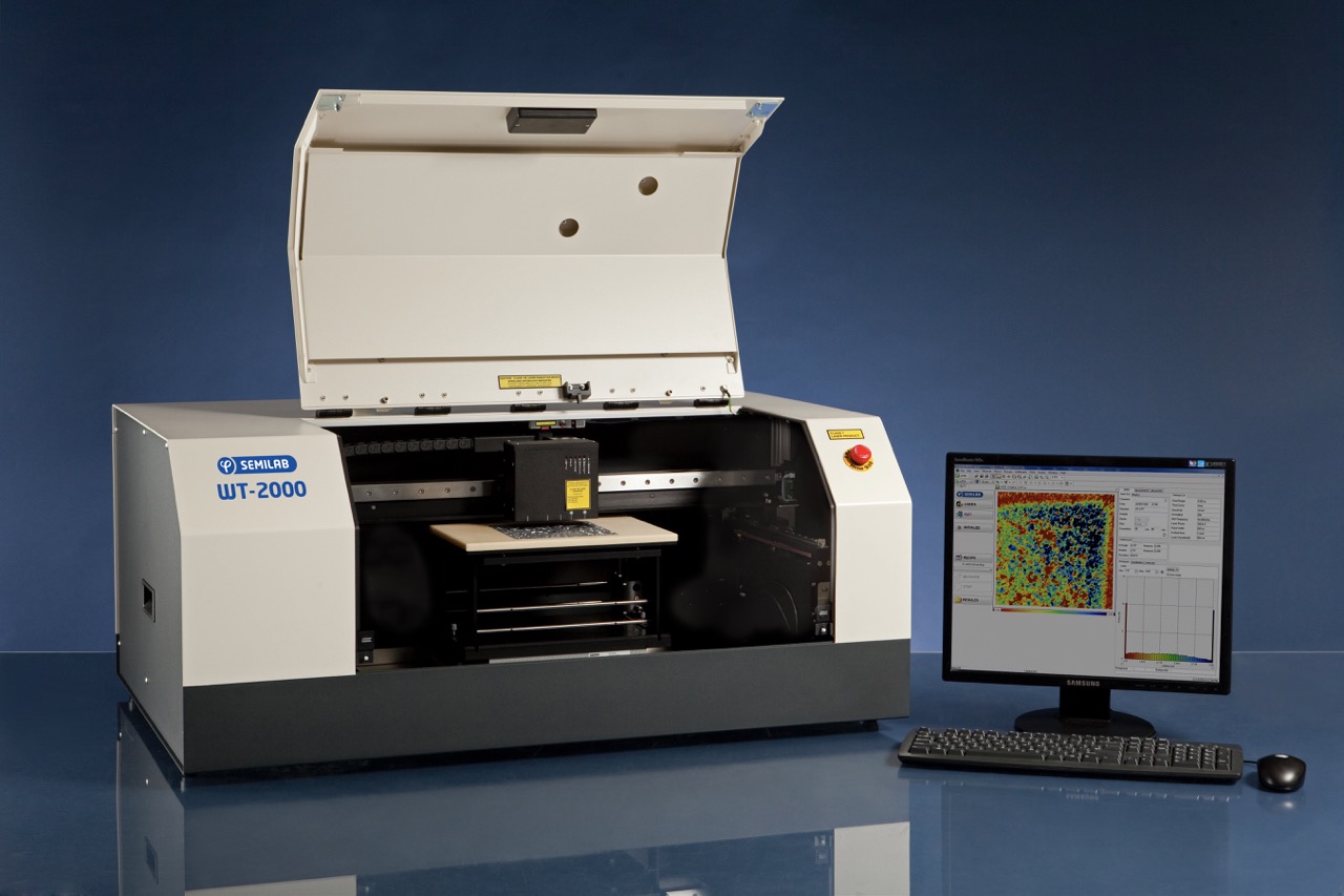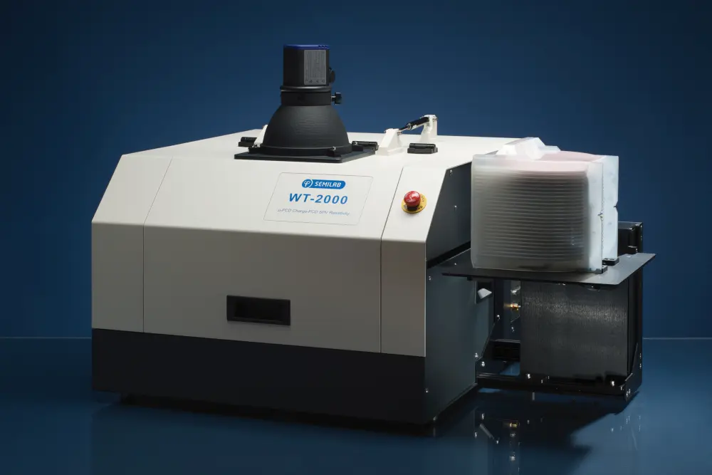
Lifetime Tester (WT) systems are advanced and versatile measurement platforms designed to perform a wide range of material characterization tasks, including carrier lifetime measurement, resistivity mapping, metal contamination detection, and other critical semiconductor property evaluations. These systems combine multiple measurement techniques and come with all accessories necessary for mapping, to deliver comprehensive wafer analysis for both research and industrial applications.
Each system can be configured based on the user’s requirements by adding measurement capabilities and automation capabilities described below. Get in touch and find your perfect WT-2000 configuration!
• Carrier Lifetime Measurement (eg.PCD techniques): Determining the effective minority carrier lifetime, a key indicator of material quality and defect density, crucial for both silicon and compound semiconductor substrates, eg. SiC.
• Contamination Monitoring with Surface PhotoVoltage technique (SPV)
• Resistivity Mapping: Non-contact (eg. Eddy) and contact (4pp) methods to map resistivity variations across the wafer surface.
Sheet Resistance Measurement (eg. JPV): Essential for assessing electrical uniformity and doping profiles on semiconductor wafers and solar cells.
• Quality Control: Robust and precise monitoring of wafer and solar cell quality throughout production lines.
• Multi-Method Capability: Enables use of various measurement principles within one system to suit different material types and characterization needs.
• Contamination monitoring with multiple different measurement methods, eg. µ-PCD, c-PCD, and offering different wavelength laser options tailored for different materials.
• Crystal defect detection
• Key feature of SPV is bulk Fe detection, and charge carrier diffusion length measurement
• Implant process monitoring with JPV sheet resistance measurement
• Electrical characterization with contact (4pp) and non-contact (Eddy) methods for bulk and thin film applications
• Automation software with SECS/GEM communication option
• High Sensitivity & Accuracy: Critical for identifying defects and contamination affecting carrier lifetime and device performance
• Flexible Application: Suitable for research and production environments, supporting wafers from laboratory samples to industrial-scale manufacturing
• Comprehensive Data Analysis: Integrated software for mapping with all offered metrologies, analysis, and reporting facilitates rapid process optimization and quality control